E77 . lab 3 : laying out simple circuits Layout nor input gate Figure 4.10 from 4. combinational cmos logic circuits cmos logic
CMOS NOR gate | Details | Hackaday.io
Draw 2 input cmos nor gate and using equivalent inverter approach and Cmos logic gate input nor combinational circuits two Cmos input
Gate nor cmos layout input magic hackaday io version
Transistor cmos schematic gate input nor structure expressionM02 lec09 cmos 3 input nor gate stick diagram Nor gate(2 input) layoutNor gate input cmos using inverter draw.
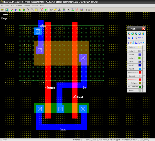
Nor layout cmosNor gate diagram stick input cmos Cmos nor gateExperiment 2 layout of 2 input cmos nor gate using microwind.

Solved i. 2. draw the cmos transistor level schematic of a
Nor gate nand cmos gates presentation ppt powerpointLayout design for cmos 2 input nor gate .
.


Layout design for CMOS 2 input NOR gate | Download Scientific Diagram

Solved I. 2. Draw the CMOS transistor level schematic of a | Chegg.com

e77 . lab 3 : laying out simple circuits
NOR Gate(2 input) layout | All For Students

Draw 2 input CMOS NOR gate and using equivalent inverter approach and

Figure 4.10 from 4. Combinational Cmos Logic Circuits Cmos Logic

PPT - NAND and NOR Gates PowerPoint Presentation, free download - ID

M02 Lec09 CMOS 3 Input NOR Gate Stick Diagram - YouTube