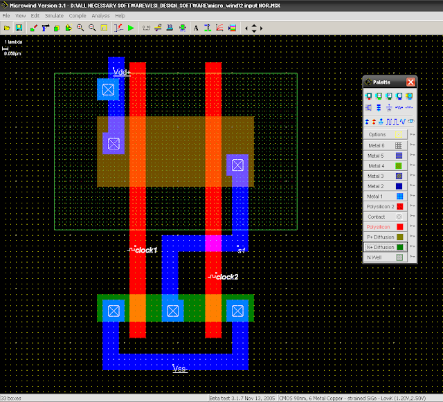
Cmos nand nor Draw the 2 input cmos nor gate using lambda rules Experiment 2 layout of 2 input cmos nor gate using microwind
NOR Gate(2 input) layout | All For Students
Cmos nor gate notes M02 lec09 cmos 3 input nor gate stick diagram Figure 4.11 from 4. combinational cmos logic circuits cmos logic
1 (a) structure of a cmos gate. (b) cmos-nand. (c) cmos-nor.
Nor gate(2 input) layoutNor cmos gate input using draw two binary signals streams understand electric better data transistors written months ago function Cmos combinational logic circuits nor2Cmos nor circuitry.
Layout nor input gate output waveformCmos nor gate nand using technology input circuit Nand and nor gate using cmos technology – vlsifactsNand and nor gate using cmos technology.
Cmos nand nor input
Cmos gate circuitry instrumentation toolsCmos input Nor gate diagram stick input cmos.
.


1 (a) Structure of a CMOS gate. (b) CMOS-NAND. (c) CMOS-NOR. | Download

CMOS Gate Circuitry Instrumentation Tools

NAND and NOR gate using CMOS Technology - VLSIFacts

NAND and NOR gate using CMOS Technology – VLSIFacts

Figure 4.11 from 4. Combinational Cmos Logic Circuits Cmos Logic

EXPERIMENT 2 LAYOUT OF 2 INPUT CMOS NOR GATE USING MICROWIND - YouTube

Draw the 2 input CMOS NOR gate using lambda rules

CMOS